Status Report - GREEN
Display & Multiplexer
background
In digital logic, A multiplexer is the logical implementation of a single pole, N position switch. In this project, we'll be using the 74LS174 multiplexer, a 1 of 8 multiplexer. This means that one output (Z) will be selected from any of the eight inputs (I0 to I7) by a set of 3 bit binary selectors (S0 to S2) in combination with ENABLE wired to low (Figure 1a).
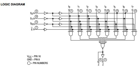
Figure 1: 74LS151 Logic Diagram
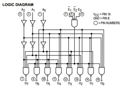
Another useful device is the 74LS138 1 of 8 Decoder. The decoder is essentially the opposite of a multiplexer, a set of 3 bit binary selectors are enabled to select an output, instead of an input (Figure 1b). This device will be used to control the power for each 7-segment display.
System description
Four of the 74LS151 multiplexers are used in this digital clock system (Figure 2). Each of these multiplexers will receive one bit of the digits (total of four bits, one per multiplexer) from the registers in order by the significance of the digits stored in the registers (Green Box). The 3 bit binary selectors of these multiplexers are synced with one another as well as the decoder by a MOD-4 counter timed with a 1kHz clock (Red Box). The counter and the decoder cycles through the displays while counter and the multiplexers cycles through the digits in sync. In combination, this enables the 7-Segments to display any numbers that's stored in the register
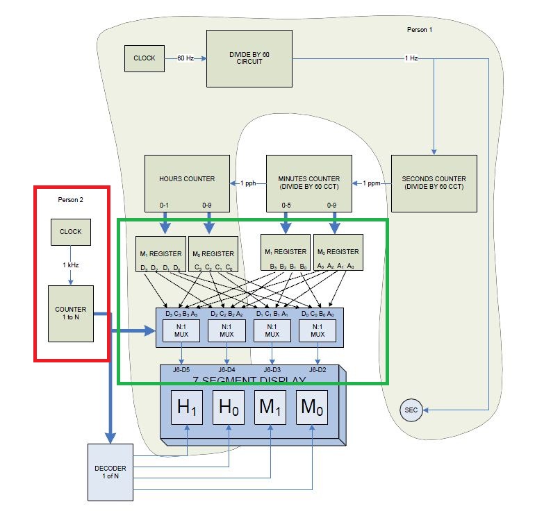
Figure 2: System Block Diagram
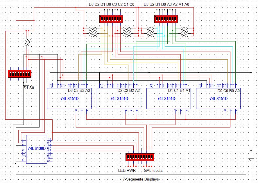
Figure 3: Circuit Diagram
Tests and results
Test Plan
The multiplexers are wired to switches to simulate the registers and the decoder. By turning on and off the switch controlling the decoder and the multiplexers, it should be possible to cycle through each of the display via the three bit selector and display the according digits stored in the simulated registers. For testing purposes, the switches are configure to display 4 and the most significant (Hour1) down to 1 at the least significant (Minute0) (Figure 4).
X indicates off, 0 low and 1 is high.

Figure 4: Expected Output
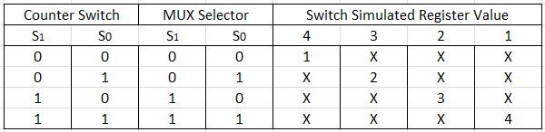
Test 1
In the first test, nothing was showing on the 7-segment display.
After a quick inspection of the circuit, I found several rows of ground and power of the multiplexer not connected at all.
In the first test, nothing was showing on the 7-segment display.
After a quick inspection of the circuit, I found several rows of ground and power of the multiplexer not connected at all.
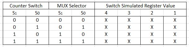
Figure 5:Test 1
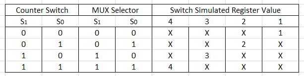
Test 2
Fixed grounding and power issues.
Display seems to be reversed...
Fixed grounding and power issues.
Display seems to be reversed...
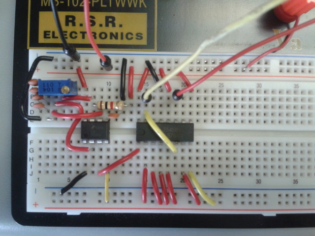
Test 3
Switched selector wires, obtained expected results
Switched selector wires, obtained expected results
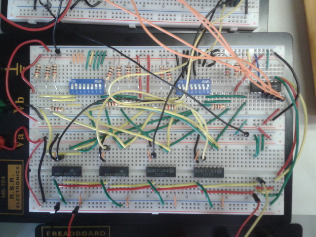
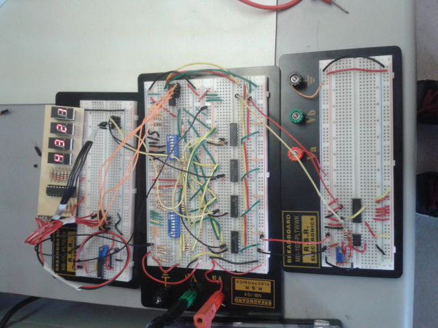
Final wiring with decoder and counter implemented
|
|
More information on counters HERE
Conclusion
The multiplexer and display system is successful with the implementation of the 1kHz clock to control the display's refresh rate. For future endeavers, I would use more colours for a more consistent wiring to keep the proto-board more readable.
The final test results shows that the chip are working as demonstrated in the datasheets, the multiplexer are wired corrected to the simulated registers and confirm the 1kHz clock functionality as the display refresh timer
The final test results shows that the chip are working as demonstrated in the datasheets, the multiplexer are wired corrected to the simulated registers and confirm the 1kHz clock functionality as the display refresh timer
